Introduction
The ever-growing demand for faster, smaller, and more efficient electronic devices has fueled the semiconductor industry‘s relentless pursuit of innovation. One crucial technology at the heart of semiconductor manufacturing is Extreme Ultraviolet Lithography (EUVL) to achieve smaller feature sizes with higher resolution, leading to miniaturized devices. Researchers and companies across the globe are focusing on developing novel Extreme UV (EUV) photoresist materials that support EUVL patterning at nanometer-scale resolutions and improve the performances of semiconductor devices. [1], [2], [3]
Lithography is a crucial step in semiconductor fabrication, where patterns are transferred onto wafers to create integrated circuits and other microstructures. Traditional lithography relies on deep ultraviolet light, but as integrated circuits reach single-digit nanometre scales, EUV lithography becomes imperative. EUV light operates at wavelengths around 13.5 nanometres, enabling the printing of significantly smaller features with high precision. EUV photoresists are light-sensitive materials utilized in the semiconductor manufacturing process, particularly in advanced lithography techniques. These materials must withstand high-energy EUV photons and provide high-resolution patterning capabilities. Some challenges for developing EUV photoresist materials are that they need to be highly sensitive to the short wavelengths, achieving high resolution is essential for producing intricate and small-scale patterns under 3nm, minimizing line-edge roughness, and outgassing (contamination) creates issues for manufacturers in maintaining production.[2], [4], [5]
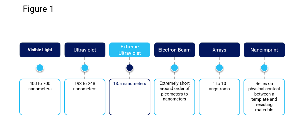
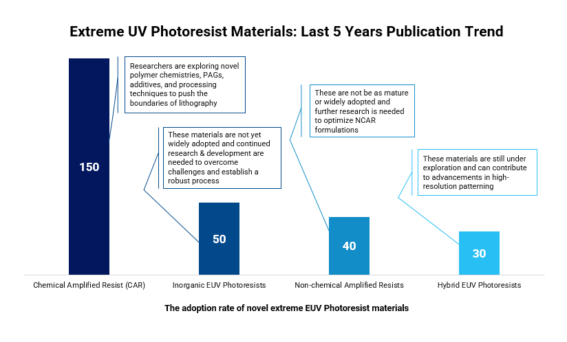
These innovative materials are often classified as Chemically Amplified Photoresists (CARs), Non-Chemical Amplified Resists, Inorganic EUV Photoresists, and Hybrid EUV Photoresists depending on their formulations or compositions. When exposed to EUV light, they undergo chemical or physical changes, enabling the accurate transfer of patterns onto surfaces.[2],[6]
Understanding Extreme UV Photoresist Material
EUV photoresist materials are light-sensitive substances that undergo chemical changes when exposed to high-energy EUV photons. EUV photons generate photoacids from a photosensitive compound. This acid catalyzes a deprotection reaction in the resist polymer, making it more soluble in the developer solution. The amplified reaction enhances sensitivity and enables high-resolution patterning. As semiconductor nodes advance to smaller scales, maintaining resolution, sensitivity, and pattern fidelity becomes more complex and challenging. Research is ongoing to develop new materials, mechanisms, and processing techniques to address these challenges and enable further miniaturization. [2], [4], [6]
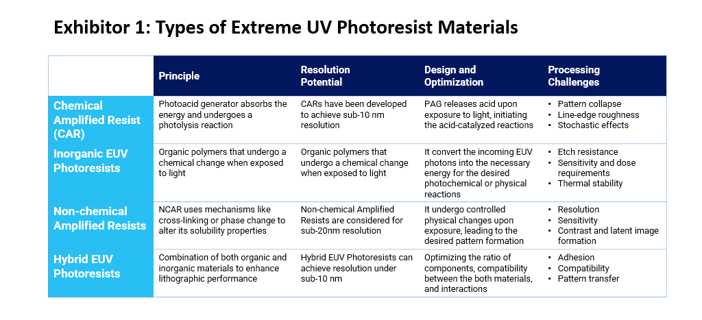
● Chemical Amplified Resist Chemically amplified photoresists are the most commonly used EUV photoresists. They employ a photoacid generator (PAG) that produces acid upon exposure to EUV photons. This acid catalyzes a chemical reaction in the resist, leading to the dissolution of the exposed regions during the development process. CARs are known for their high sensitivity, making them suitable for low-dose EUV exposure and improving throughput during semiconductor manufacturing. They may find applications in optical devices, displays, and advanced packaging. [2], [7], [8]
● Inorganic EUV Photoresists Inorganic photoresist materials with different EUV absorption coefficients and high etching are important to solve some existing problems. Therefore, many researchers have begun to study the use of inorganic materials in the field of photoresists. These materials differ from organic CARs as they are composed of inorganic materials, such as metal oxides or metal-containing compounds. They work by applying the metal oxide system with acrylic acid as the organic ligand to EUV lithography. Inorganic photoresists are expected to offer higher thermal stability and reduced outgassing than their organic counterparts. They may find applications in extreme environments or specialized semiconductor processes. [2], [7], [8]
● Non-chemically Amplified Resists Unlike CARs, non-chemically amplified photoresists do not rely on acid-catalyzed reactions. Instead, they directly undergo a photolytic reaction upon EUV exposure, resulting in a change in solubility. These materials often require higher doses of EUV light for patterning and are being explored for specific applications and process requirements. [2], [7], [8]
● Hybrid EUV Photoresists Hybrid EUV photoresists combine organic and inorganic elements to leverage the advantages of both material types. These materials work by selecting the resins selected for the purification step after the ligand exchange reaction as polystyrene resins functionalized with tertiary amines, piperidine, and dimethylamine. These materials aim to provide enhanced sensitivity, resolution, and thermal stability, addressing some of the limitations of purely organic or inorganic photoresists. [2], [7], [8]
Key Challenges in EUV Photoresist Development
● EUV Sensitivity Sensitivity is one of the key challenges of EUV lithography; developing and optimizing photoresist materials that effectively absorb and react with EUV light to produce precise patterns on semiconductor wafers is difficult. EUV photons are scarce and expensive, necessitating photoresist materials with high sensitivity to achieve an adequate throughput of 100 to 120 wafers per hour during manufacturing.[9], [10]
● Resolution and LER As feature sizes reduce, maintaining high resolution without excessive line-edge roughness (LER) becomes problematic. An important potential source of LER for EUV resists is photon shot noise due to the high photon energy. The LER challenge involves minimizing irregularities or roughness along the edges of the developed photoresist lines that form the transistor features. Excessive LER can lead to variations in transistor performance and reduced chip yield. The manufacturers need to optimize the photoresist formulation and process conditions to achieve an LER of 2 nm but a sensitivity of only 70 mJ/cm and smoother, more precise edges on the transistor features. [2], [9]
● Outgassing The outgassing problem in EUV lithography refers to releasing volatile organic compounds (VOCs) or other materials from the photoresist during exposure to EUV light. These outgassed materials potentially contaminate the surrounding environment, including the optics and mirrors used in the EUV lithography equipment. Contamination reduces equipment performance and production yield, alongside increasing maintenance requirements. Controlling and minimizing outgassing is critical to maintaining the reliability and efficiency of the entire EUV lithography process.[9], [11]
● Thermal Stability EUV exposure generates considerable heat, demanding stable photoresist materials under high-energy conditions. Many applications demand coatings with excellent thermal stability. Most commercially available removers rapidly dissolve resist layers after thermal loads of up to 130°C. [9], [12]
Promising Advancements in Novel EUV Photoresist Materials
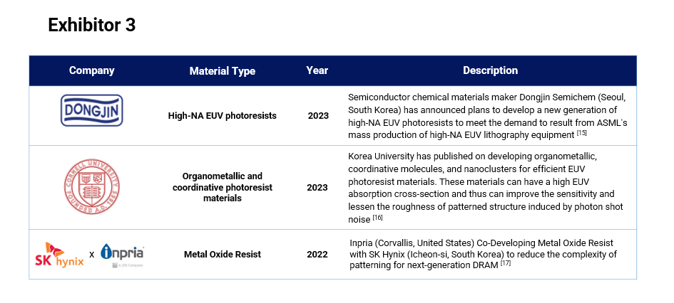
● High Sensitivity, Low Dose Materials Researchers are exploring innovative chemically amplified photoresists that react strongly to EUV photons even at lower doses, improving throughput to 100 wafers per hour and reducing manufacturing costs. [1o], [13], [14]
● Improved Resolution and LER Control Novel materials such as chemically amplified and inorganic resists are designed to mitigate LER while maintaining high-resolution patterning capabilities. Advanced chemical atomic resist compositions and unique polymer structures play a vital role in achieving higher sensitivity to EUV light, improving contrast, and reducing LER below 2nm.[13], [14]
● Reduced Outgassing The development of low-outgassing photoresists ensures cleaner EUV exposure, resulting in a higher yield and improved semiconductor device reliability. Reducing outgassing is crucial to maintaining the cleanliness and integrity of the EUV lithography process, which is highly sensitive to contaminants. Semiconductor manufacturers collaborate closely with material suppliers and equipment manufacturers to ensure that the photoresists and other materials used in the EUV lithography process meet stringent outgassing requirements and contribute to producing high-quality semiconductor devices.[11], [13], [14]
● Thermal Stability Solutions To tackle the thermal challenges of EUV lithography, researchers are bringing engineering materials with enhanced thermal stability, allowing for more prolonged exposure times without compromising performance. [12], [13], [14]
Collaboration and Future Prospects
Developing and optimizing novel EUV photoresist materials requires collaboration between semiconductor manufacturers, material suppliers, and research institutions. The semiconductor industry’s pursuit of next-generation devices relies on the continual advancement and refinement of EUV lithography technology. [14], [18]
The successful implementation of novel EUV photoresist materials will unlock numerous possibilities for semiconductor technology. Smaller and more powerful devices will revolutionize various sectors, including data centers, healthcare, automotive, and artificial intelligence. The impact is not only limited to traditional computing, allowing semiconductor manufacturers to produce chips with smaller feature sizes. This leads to higher transistor density, improved performance, and lower power consumption in electronic devices. It also enhances the capabilities of semiconductor devices, enabling the production of advanced processors, memory devices, and sensors that drive technological innovation in various industries [14], [18], [19]
Conclusion
Novel Extreme UV photoresist materials represent a crucial stepping-stone in the relentless drive to enhance semiconductor technology. The ability to print ever smaller and more precise features on semiconductor wafers is vital to meeting the demands of the digital age. Collaborative research and development in this field promise a bright future for the semiconductor industry, ensuring the continuous evolution of electronic devices that empower and enrich our lives.
Developing novel EUV photoresist materials requires collaboration among material scientists, chemists, physicists, and engineers. Material suppliers, semiconductor manufacturers, and research institutions work in tandem to design, characterize, and test these materials under demanding EUV exposure conditions.
The field of EUV lithography and photoresist development is continuously evolving. Researchers are exploring a wide range of material innovations, including inorganic resists, nanostructured materials, and hybrid polymers. As the semiconductor industry strives for even greater levels of miniaturization and performance, the pursuit of novel EUV photoresist materials remains an active area of research and innovation.
Learn more about how we can empower your organization in the dynamic world of Semiconductors by emailing us at contact@iebrain.com.
About Ingenious e-Brain : –
Ingenious e-Brain provides high-quality, customized, and cost-effective Technology Research, Business Research, and Intellectual Property Research solutions to industry leaders, and innovative companies across the globe. Innovation, knowledge, and transparency form the basis of our company’s mission and vision. Along with cost benefits, we provide highest quality results ensuring fool-proof confidentiality and security. We are an ISO certified company with offices in India and USA.
Ingenious e-Brain has a strong team of analysts, and subject matter experts with domain proficiency which is devoted to help clients grow. Our highly qualified professionals offer tailored, value-added and cost-effective services to our clients. We believe in building long term relationships with our clients who include national and international corporations, Fortune 500 companies, world’s leading research institutes and universities as well as independent inventors.

